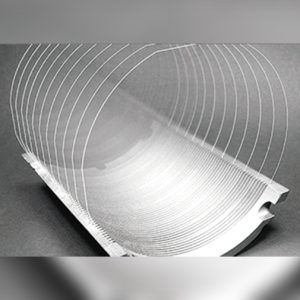

Advantage:
● High economic efficiency, hundreds and thousands wafers can be cut at a time;
● Can cut silicon ingots up to □230mm×L900mm;
● Small depth of crystal defects;
● Few geometric defects (TTV, bowing, deviation, etc.)
● Sawing thinner wafers;
● Reducing the cost of solar cells;
● CE Conformity.